

About a week ago, I caved in and decided to spring for one of those huge, high-power USB-C power delivery hubs that have sprung up in the past couple of years.
Given that on a large shoot day, I often have a laptop, two or more camera batteries, a gimbal, two different drone controllers, a rack of drone batteries, two FPV goggle batteries, and a selection of other miscellaneous USB-charged devices, I’d finally had enough of playing musical chairs with a handful of standalone USB chargers that all supported different charge standards trying to get the most efficient charging routine down. I’d been bitten by this before, in situations where I literally could not go to bed until putting the last of the batteries on to charge, necessitating an extra-large coffee the next morning.
Note: All products mentioned in this article were purchased by me, with my own money. The manufacturers involved have neither solicited nor endorsed this piece and have not been afforded any prior restraint or review.

After doing some cursory research and coming to the conclusion that if I was going to spend upwards of $150 anyway, I might as well get the biggest, baddest one I could, I settled on the Ugreen Nexode 300W hub. At a list price of $270, it actually caused some physical discomfort to click the buy button for what is essentially a fancy power brick, but as long as it solved my problem, it would be worth it.
And I’m delighted to say that it has! It’s got enough ports and enough juice that I can charge all of my gear in a significantly shorter time than I had previously, in addition to not having to deal with several individual chargers all with their own compatibility specifications and power delivery limitations. I’ve since standardized my USB-C cables to a set of identical bright blue 100W cables from Kondor Blue, so I’ll never be left in any doubt as to which of the seemingly hundreds of generic black cables I have are charging compatible.
The whole experience has led me to wonder, though: what is it about this new “GaN” charge technology that enables such an improved process for taking power from the grid and putting it into my stuff? I mean, I’ve had wall-wart style chargers and power supplies since I was a kid, and we’re only now discovering that we can use a slightly different design to take what used to be a 5-watt charger for a single device, or maybe even 10 watts if you were fancy like that, and turn it into a huge, heavy brick of a thing that can seemingly power a modestly-sized aircraft carrier?
Peruse your favorite online marketplace and you’re sure to see hundreds of devices marketed with the “GaN” prefix, so it sure seems to be a marketing buzzword. What gives?
Let There Be Light
Gallium nitride, the chemical compound behind the “GaN” moniker, is a semiconductive material that was first synthesized in 1932 at the George Herbert Jones Laboratory by reacting gallium metal and ammonia at searingly-high temperatures of between 900C and 1000C (1652F-1832F for my American brethren).
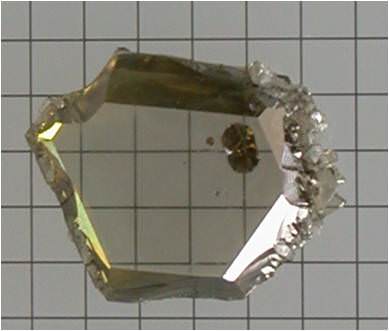
While its properties as a semiconductor were apparent, due to its highly imperfect and random crystal structure, it did not see much demand until 1972, when it was used to manufacture blue LEDs, though these LEDs were still too dim to see commercial use. That is, until 1991, when Shuji Nakamura, Isamu Akasaki, and Hiroshi Amano at Nichia Chemical patented a process to manufacture high-brightness blue LEDs using the compound, by infiltrating its crystal structure with huge amounts of magnesium metal in a process called “doping”.
As it turns out, this was a seismic moment in the consumer electronics industry. As I’m sure you know, white light can be created by combining red, green, and blue light. This is how just about every color screen you’ve ever seen actually works, even the old CRT that’s now relegated to Nintendo 64 duty in your basement, and how a camera’s sensor records color by way of a Bayer filter. The problem had been that while red and green LEDs had been available for some time, nobody had cracked the code to producing blue light from a device similar in size and design that could be combined with them in a single module.
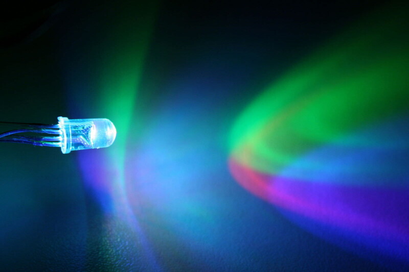
Lo and behold, that’s exactly what Nakamura-hakase and his team had done, an achievement that won them the 2014 Nobel Prize in Physics, and which paved the way for everything from small, efficient white LED flashlights to the RGB LEDs so many of us custom PC enthusiasts rely on for our bling.
GaN photonics technology has gone on to enable the development of blue lasers and the subsequent development of the Blu-Ray disc, giving movie buffs everywhere a significant upgrade in their physical data storage.
Unlimited Power…?
In recent years, gallium nitride has gained traction as a potential replacement for MOSFET transistors in electronic devices. MOSFETs, or Metal Oxide Semiconductor Field-Effect Transistors, are electronic components that can be used to rapidly switch electric current on and off.
In a nutshell, you can think of a MOSFET like an electrical dam. Because of the chemical composition and layout of the material the MOSFET is made from, applying a “control” voltage to the component can change how easily electrical current can flow through it, up to and including shutting it off completely, just as a dam can be controlled to either allow water to flow through in specific amounts, or hold it back entirely.
However, this type of transistor is affected by parasitic losses when switching on and off, due to the imperfect efficiency of the switching operation. This results both in a lowered actual power throughput and, occasionally, so much heating that in high-current applications, MOSFETs can require their own dedicated heat sinks and cooling to prevent failure.
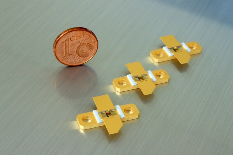
By contrast, FETs that use gallium nitride rather than silicon or metal oxides are massively more efficient, and thanks to their unique low-impedance properties, can switch between open and closed states much more quickly, alleviating two of the major hurdles in high-speed, high-power electronics. The first of these was successfully demonstrated in 1993 by a team from APA Optics, Inc. of Minnesota.
Then, in 2009, a startup known as Energy Power Conversion debuted its adapted method for producing transistors using gallium nitride as its active material rather than the silicon compounds that had been used previously, which proved that they could be made cheaply and efficiently on equipment most manufacturers already had or could modify. Later, thanks to the integration of the GaN FETs themselves, GaN-based drive circuitry, and current protection into a single circuit (helpfully called an “integrated circuit”) by HRL Laboratories of Malibu, California in 2016, GaN-based electronics have only become more widely used and commercially available, to the point we can now buy them off-the-shelf.
Who would’ve thought a charger could be so interesting?